Low MOQ for Mono-Crystalline 150W Solar Panel to Uruguay Manufacturer
Short Description:
The key to our success is "Good Product Quality, Reasonable Price and Efficient Service" for Low MOQ for Mono-Crystalline 150W Solar Panel to Uruguay Manufacturer, With the aim of "compete with good quality and develop with creativity" and the service principle of "take customers' demand as orientation", we will earnestly provide qualified products and good service for domestic and international customers.
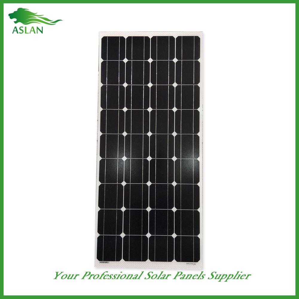
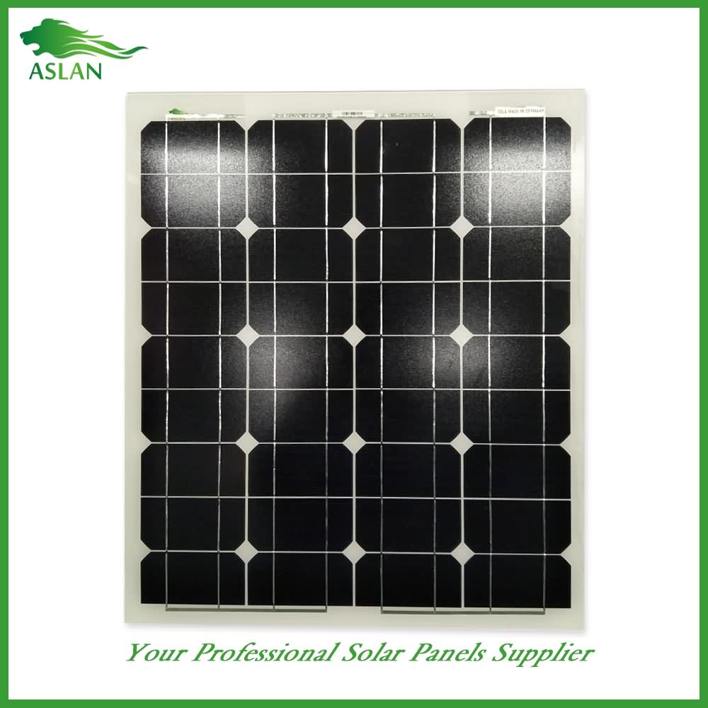
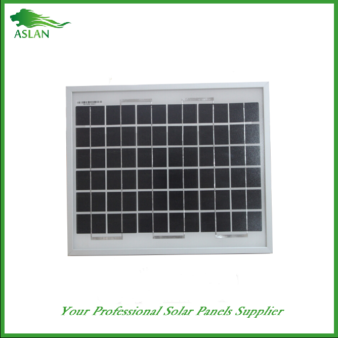
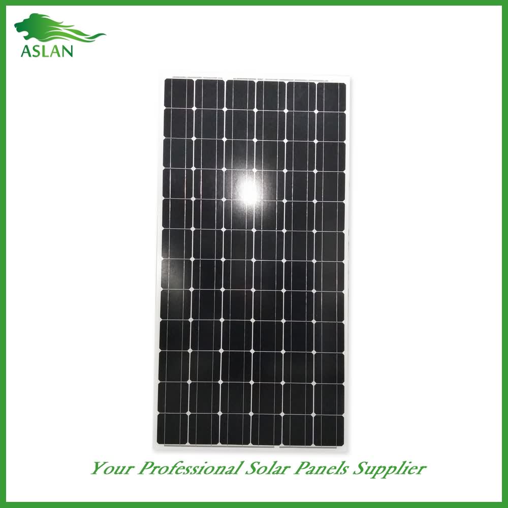
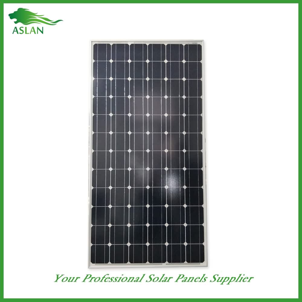
Mono-Crystalline 150W Solar Panel
Technical parameter
Maximum Power(W) 150W
Optimum Power Voltage(Vmp) 17.92V
Optimum Operating Current(Imp) 7.83A
Open Circuit Voltage(Voc) 21.86V
Short Circuit Current(Isc) 8.59A
Mechanical Characteristics
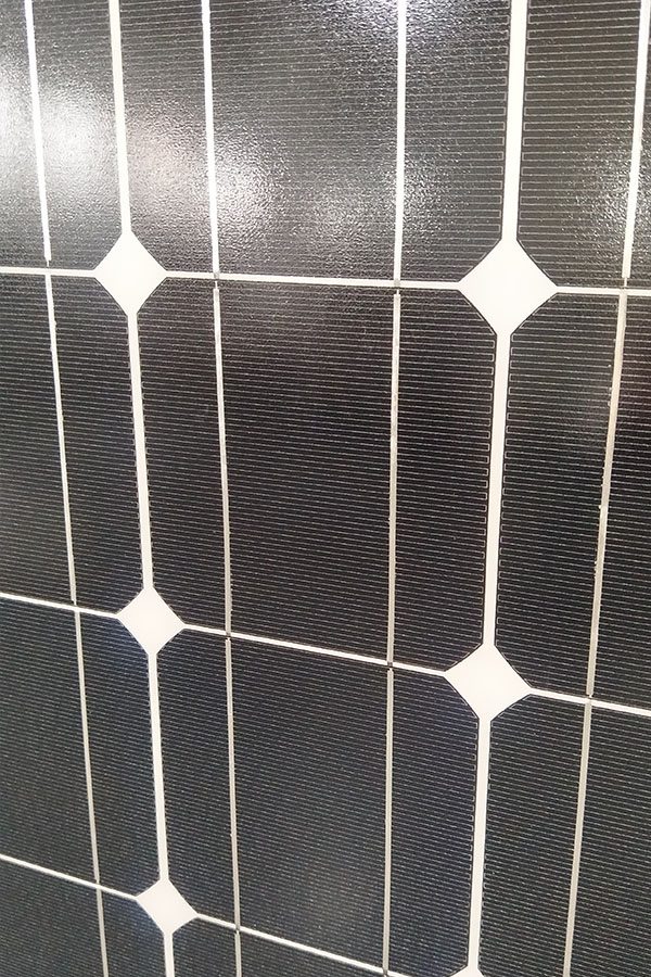
Cell Type Monocrystalline 156x156mm (6 inch)
No of Cell 36 (4x9pcs)
Dimensions 1485x668x35mm
Weight 11.6KGS
Front Glass 3.2mm,High Transmission, Low Iron,Tempered Glass
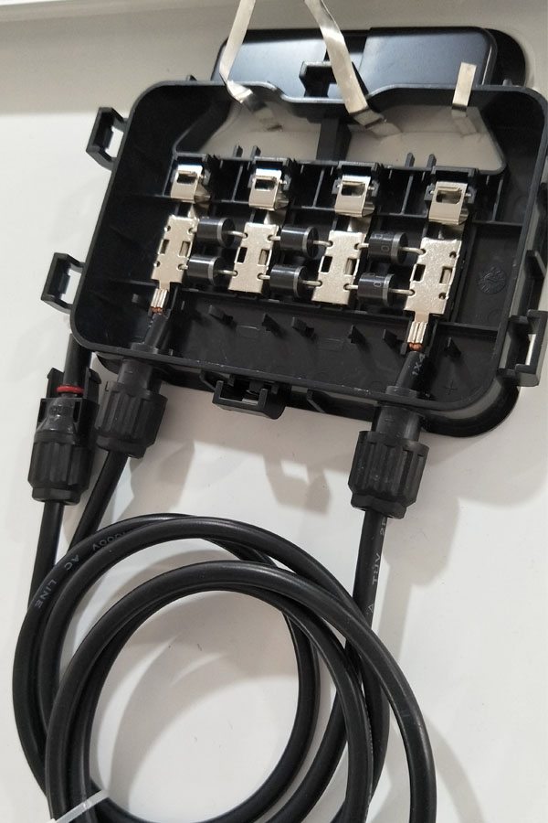
Junction box IP65 Rated
Output Cable TUV 1×4.0mm2/UL12AWG,Length:900mm
Temperature and Coefficients
Operating Temperature(°C): -40°C ~ + 85°C
Maximum System Voltage: 600V(UL)/1000V(IEC) DC
Maximum Rated Current Series: 15A
Temperature Coefficients of Pmax: -0.435%
Temperature Coefficients of Voc: -0.35%
Temperature Coefficients of Isc: 0.043%
Nominal Operationg Cell Temperature (NOCT): 47+/-2°C
Materials of solar panel
1).Solar Cell——Mono-crystalline solar cell 156*156mm
2).Front Glass——-3.2mm, high transmission, low iron, tempered glass
3).EVA——-excellent anti-aging EVA
4).TPT——-TPT hot seal made of flame resistance
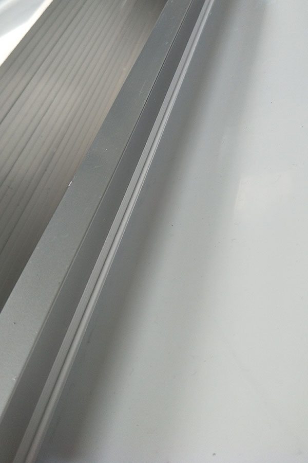
5).Frame——anodized aluminum profile
6).Junction Box——-IP65 rated, high quality, with diode protection
Superiority: high quality anodized aluminum frame, high efficiency long life, easy installation, strong wind resistance, strong hail resistance.
Features
1. High cell efficiency with quality silicon materials for long term output stability
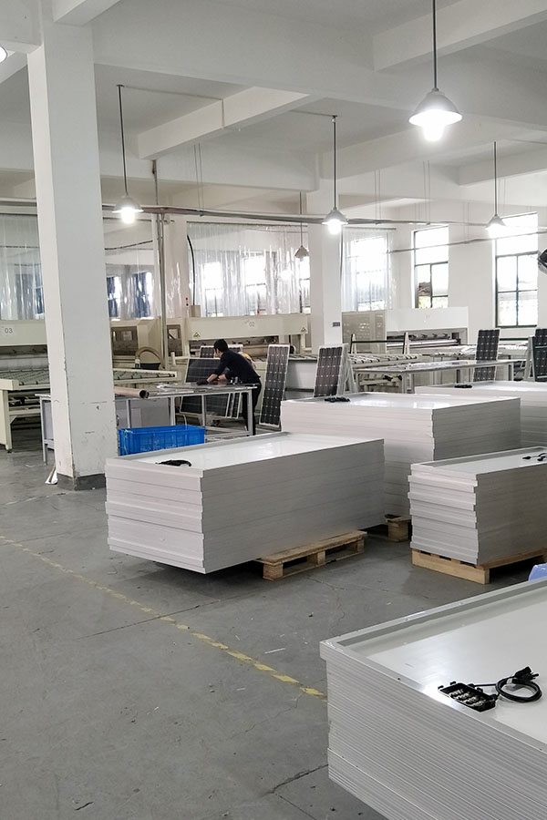
2. Strictly quality control ensure the stability and reliability, totally 23 QC procedures
3. High transmittance low iron tempered glass with enhanced stiffness and impact resistance
4. Both Polycrystalline and Mono-crystalline
5. Excellent performance in harsh weather
6. Outstanding electrical performance under high temperature and low irradiance
Quality assurance testing
Thermal cycling test
Thermal shock test
Thermal/Freezing and high humidity cycling test
Electrical isolation test
Hail impact test
Mechanical, wind and twist loading test
Salt mist test
Light and water-exposure test
Moist carbon dioxide/sulphur dioxide
Nikola Tesla Cosmic Ray Radiant Energy Receiver Solar Cell Battery Patent 1901 http://nikolateslasolar.blogspot.com Recent developments in various types of solar cells from Silicon, CIGS, CIS, CGS, CdTe, Dyes and Polymers include stacked multi-junction, concentrated solar, concentrated solar plus sterling engine, multi-junction concentrated CPV, tandem with NIR-transparent perovskite top cells, thin layer, hybrid, bi-facial, plastic, spray on, spray-coated, contact-less printed, back-side bus-bar screen-printed, back-side reflective junction, 3-D printed, dye-sensitized or double-glass, PVSC semi-transparent perovskite, GaAs plasmonic nano-particles, co-polymer fluoride for a push-pull, for thermo-chromatic function, solar layers for paint, coating and floorings, MoS2 variable band-gap 2D crystalline semi-conductors; liquid to liquid exfoliated nano-flakes, laser-induced micro-explosions, optical concentrated solar, OSCs inverted poly-fluorine dots, doping of PF dots , DSSCs panchromatic quasi-monolayers, ssDSSCs scaffold photoelectrodes, OCC hydrophyllic perovskite hydrophobicity (high carrier mobility) at 15-25) efficiency, X-ray polymer printed organic electronics, aqueous/organic dye sensitized, Fumed silica MMTMs macro-mesoporous, solar cells printed out of a printer for wallpaper, MOFs dyes for indirect band-gaps, Super-material 2D TMDCs Graphene and Selenium “Sandwich” stacked to 3D, Kesterite sol-gel, spin-coated Spiro-MeOTAD films, inject printing solar cells, Stibnite polymer chemical bath, Perovskite SSE room temperature chemical pre-cursor, stained glass, creating uniformity or filling, with anti-reflective or scattering or to facilitate light trapping, large surface areas, highly polished or amalgamated, small spark-gaps or to nano size in order to improve carrier transport or electron flow, maximize carrier recombination at donor-acceptor interfaces, maximize the pushing pressure of light, reduce light induced degradation, prevent leakage between layers, minimize series resistance and reduce magneto-resistance. June 16th 2015 ETH Zurich explains the magneto-resistive effect. In many cases modern solar cells are manufactured using Tesla Patent #577671 and #567818 November 5th 1896, Manufacture of Electrical Condensers & Coils method using vacuum chambers. April 13th 2015 Long-sought magnetic mechanism observed in exotic hybrid materials for tunable topological insulators. May 25th 2015 University of Tokyo studies defect-free topological insulators and thin film electric gating. DSSc Dye Sensitized Cell Market – Global Industry Analysis and Forecast to 2020.
SPIE 2015 Gold Medal Award recipient Nader Engheta of the University of Pennsylvania will discuss some of the technologies made possible by controlling photons and optical waves. “Materials control waves, and they can tailor, manipulate, redirect, and scatter electromagnetic waves and photons at will,” Engheta said. “Recent developments in condensed matter physics, nanoscience, and nanotechnology have made it possible to tailor materials with unusual parameters and extreme characteristics, providing fertile ground for innovation and discovery.”
Most manufacturing or amalgamation of silicon and thin-layer solar cells today use this process of using vacuum chambers, with heat, air pressure, magnetic pressure, electro-deposited, thermo-magnetic, harmonics, redox, chemically doped, chemically catalyzed, sol–gel and hydrothermal methods, temperature and pressure with solvents, graded lattice (GaInNAs), template stripping method for an omnidirectional nano-photonic solar selective absorber, DSSS doped photo-anode silver nano-particles (for improved interfacial charge transfer and retarded charge recombination process), DSS bio-nano process, DSSCs panchromatic quasi-monolayers, Blu-ray Discs nano-structure photon trapping making solar cells more efficient, InGaN nano-dots covered with ITO films, night-time polymer OPV Ni-ITO, metallic doping, encapsulated coating for hydrogen electrolysis, OCC perovskite morphology method, PEC surface states in water splitting, X-ray printed organic polymers, aqueous/organic sensitizers, ssDSSCs electro-spinning scaffold photoelectrodes, MMTMs spray drying and fumed , OCCs back-electrode thermal evaporated, spin coated nano-sphere lithography, Kesterite Sol–Gel tuning and Selenization Process , Pin holes be gone with spin coated and vacuum evaporation, inkjet printing process’ deposit of buffer and TCO layers, room temperature solution grown perovskite nano-wire lasers, 3D printed light traps, Perovskite doped chlorine and iodine, all generally amalgamated. processes to impress the junctions and form the stacked, pyramid, dome, cubic, crystalline and buss-bar structures.
UPDATE: This oven hit 340 degrees!
Hi,
This is my new solar oven.
The other day I baked 5 potatoes in it and the taste is incredible.
It was 60 deg outside and within 2 minutes the temp rose to 100 deg.
After fifteen minutes the temp was 180 deg and within an hour it reached 240 deg!
I was very excited to break the 212 temp.
This design is called the 60/40 solar oven. 40 degrees is the angle of the side reflectors (The ones in between the straight edges.) 60 degrees is the angle that the reflectors sit in reference to the oven itself. NO aerosol paint used inside the oven, only heavy foil and Elmers natural glue.
I’m always happy to hear from anyone who wants to write me.
:O)
